Data analysis sheet for wafer bond strength
measurements
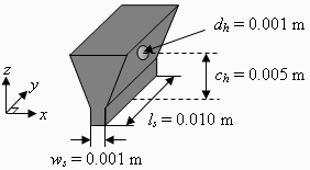
a)b)
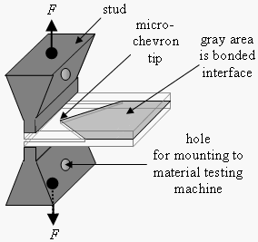
Figure WBS.1.1. a) Studs mounted to a
micro-chevron test structure and b) stud dimensions
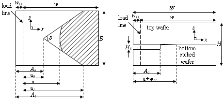
a)
b)
Figure WBS.1.2. A micro-chevron test structure
showing a) a top view and b) a cross section
To obtain
the following measurements,
consult SEMI standard test
method MS5 entitled "Test
Method for Wafer Bond Strength
Measurements Using Micro-Chevron
Test Structures."
IDENTIFYING INFORMATION:
date data taken (optional)
=
/
/
Table 1 -
Restricted
Configuration
for Sample Assembly
Description
Wafer
materials:
1
bottom wafer =
bottom wafer material
2
top wafer =
top wafer material
Micro-chevron
dimensions:
3
b =
micro-chevron angle
4
A0 =
minimum mouth length
5
A1 =
maximum mouth length
6
h1 =
top wafer thickness
7
h2 =
bottom wafer thickness
8
H =
test structure height
9
HK =
etch depth
10*
B =
width
11*
W =
length
Stud
dimensions:
12*
ws =
width of stud
13
ls =
length of stud
14
dh =
hole diameter in stud
15
ch =
distance of center of hole in stud
to bonding surface
Minimum value of the geometry
function:
16*
Ymin =
minimum value of the geometry
function(use 72.493 for the restricted configuration)
* The four starred items in this
table are required for the calculations in the Preliminary
Estimates Table.
Table 2 - Preliminary
INPUTS
Description
Wafer
specifications:
1
source =
source of silicon
2
orient =
(anisotropic)
(anisotropic)
(anisotropic)
(anisotropic)
(isotropic)
crystal orientation
3
ρ
=
Ω-μm
bulk resistivity
4
pol =
single- or double-side polished
5
method
=
method of
wafer bonding
6*
E =
GPa
= 0 (i.e., enter 0, if an
anisotropic material, such as mono-crystal silicon, is
used) = Young's modulus (if an isotropic material is
used)
7*
ν =
= 0 (i.e., enter 0, if an
anisotropic material, such as mono-crystal silicon, is
used) = Poisson's ratio (if an isotropic material is
used)
8*
Einit
=
GPa
= plane strain elastic modulus
(if an anisotropic material, such as mono-crystal
silicon, is used) = 0 (i.e., enter 0, if an isotropic
material is used)
9*
σEinit
=
GPa
= the one sigma uncertainty of the value ofE
(if an anisotropic material, such as mono-crystal
silicon, is used) = the one sigma uncertainty of the
value of
E (if an isotropic material is used)
10*
Gcwbinit =
J/m2
initial estimate for critical
wafer bond toughness
Environmental
conditions:
11
temp =
°C
temperature
12
hum =
%
relative humidity
Instrumental
specifications:
13
cert
=
N
certified value of load cell
14
σcert
=
N
the one sigma uncertainty of the
value of the load cell
15
rate =
mm/sec
displacement rate
Some sample
standard deviations:
16
σW
=
mm
the one sigma uncertainty of the
value of W
17
σB
=
mm
the one sigma uncertainty of the
value of B
18
σwLL
=
mm
the one sigma uncertainty of the
value of wLL
19
σYmin
=
the one sigma uncertainty of the
value of Ymin
Measurement and
calculation results:
20
Fmax
=
N
maximum fracture force
21
σFmax
=
N
the one sigma uncertainty of the
value of Fmax
* The five starred items in
this table are required for the calculations in the Preliminary
Estimates Table.
Table 3 - Preliminary
ESTIMATES*
Description
1
E=
GPa
plane strain elastic modulus
If an anisotropic material, such
as mono-crystal silicon, is
used,
E=
Einit
.
If an isotropic material is
used,
E = E / (1-ν2).
2
σE
=
GPa
the one sigma uncertainty of the value ofE
If an anisotropic material, such as mono-crystal
silicon, is used, σE =
σEinit .
If an isotropic material is used,
σE =
σEinit
/ (1-ν2).
3
certapp
=
N
= B SQRT[Gcwbinit
E w]
/ Ymin
(an approximate
value for cert)
* The nine starred items in the first two tables are required for
the calculations in this table.
OUTPUTS:
1.
Critical wafer bond toughness =
Gcwb =KC2
/
E
= J/m2
(USE THIS VALUE) where KC = Fmax (Ymin) / [B SQRT(w)]
=
MPa m1/2
Report the results as follows: Since it can be assumed that the
estimated values of the uncertainty components are approximately uniformly
or Gaussianly distributed with approximate combined standard
uncertainty uc, the
critical wafer bond toughness is believed to lie in the
interval Gcwb ±
uc (expansion factor
k=1) representing a level of confidence of approximately 68 %.
Modify the input data, given the information supplied in any flagged
statement below, if applicable, then recalculate:
1.
Please fill out the entire form.
2.
For the restricted configuration, Ymin
should equal 72.493.
3.
The value for
ρ
should be between 100
Ω-μm and 500
Ω-μm.
4.
For an anisotropic material, the value entered for E
should be 0. For an isotropic material, the
value for E should be between 50 GPa and 300 GPa.
5.
For an anisotropic material, the value entered for
ν
should be 0. For an isotropic material, the
value for
ν
should be between 0.0 and 0.5.
6.
For an anisotropic material, the value
for
Einit should be between 50 GPa
and 300 GPa. For an isotropic material, the value
entered for
Einit should be 0.
7.
The value for
σEinit
should be between 0.0 GPa and 0.1E
or 0.1Einit.
8.
The value for Gcwbinit
should be between 0.10
J/m2
and 10.0
J/m2.
9.
The value for temp
should be between 22 °C
and 24
°C, inclusive.
10.
The value for
hum should be between 43 %
and 47 %, inclusive.
11.
The value for cert
should be between 1 N and 100 N.
12.
The value for
σcert
should be between 0.0Nand 0.01cert.
13.
The value for rate should be
between 0.05 mm/sec and 0.50 mm/sec.
14.
The value
for
σW
should be between 0.0 mm and 0.5 mm.
15.
The value
for
σB
should be between 0.0 mm and 0.5 mm.
16.
The value
for
σwLL
should be between 0.0 mm and 0.3 mm.
17.
The value
for
σYmin
should be greater than 0.0 and less than or equal to 0.01Ymin.
18.
The value
for Fmax
should be between 0.0 N and cert.
19.
The value
for
σFmax
should be between 0.0 N and 0.05Fmax.
20.
The value
for Gcwb
should be between 0.10 J/m2 and 10.0
J/m2.
21.
The value
for KCshould be between 0.05 MPa m1/2 and 0.50
MPa m1/2.
22.
The value
for uc
should be between 0.0
J/m2
and 0.1 J/m2.
23.
The values
for uFmax,
uB, uw, uYmin,
and uE should be between
0.0 J/m2 and 0.1 J/m2.

 b)
b)