Data
analysis sheet for thickness
measurements in a commercial CMOS
process.
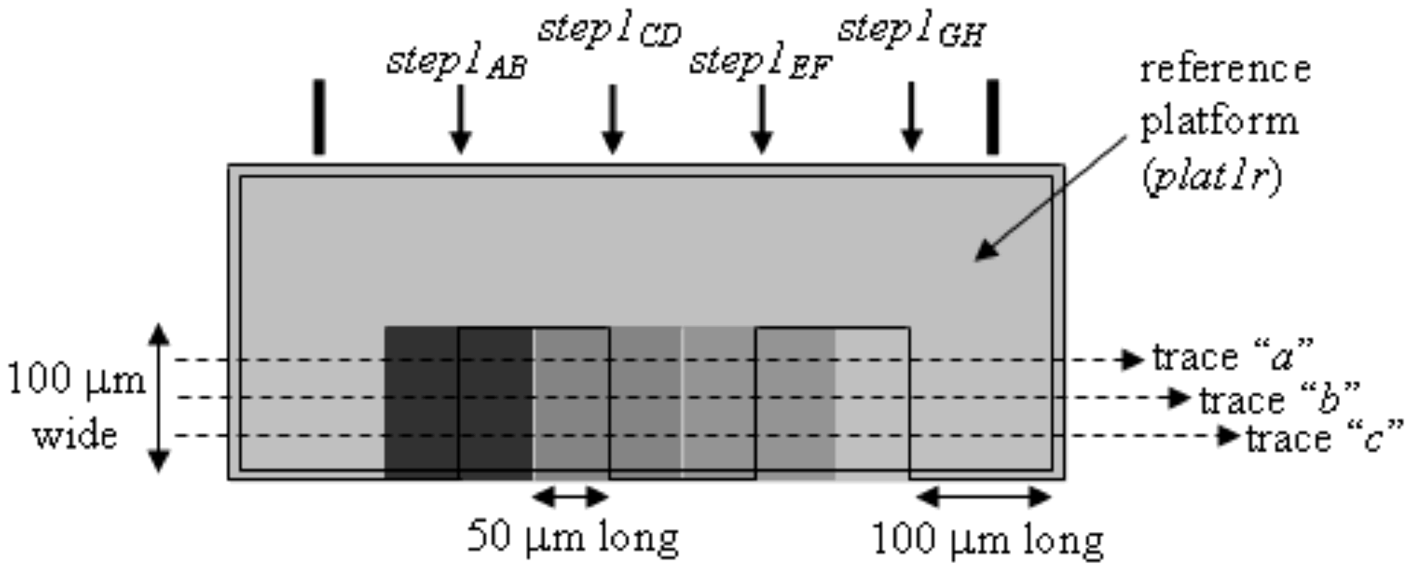
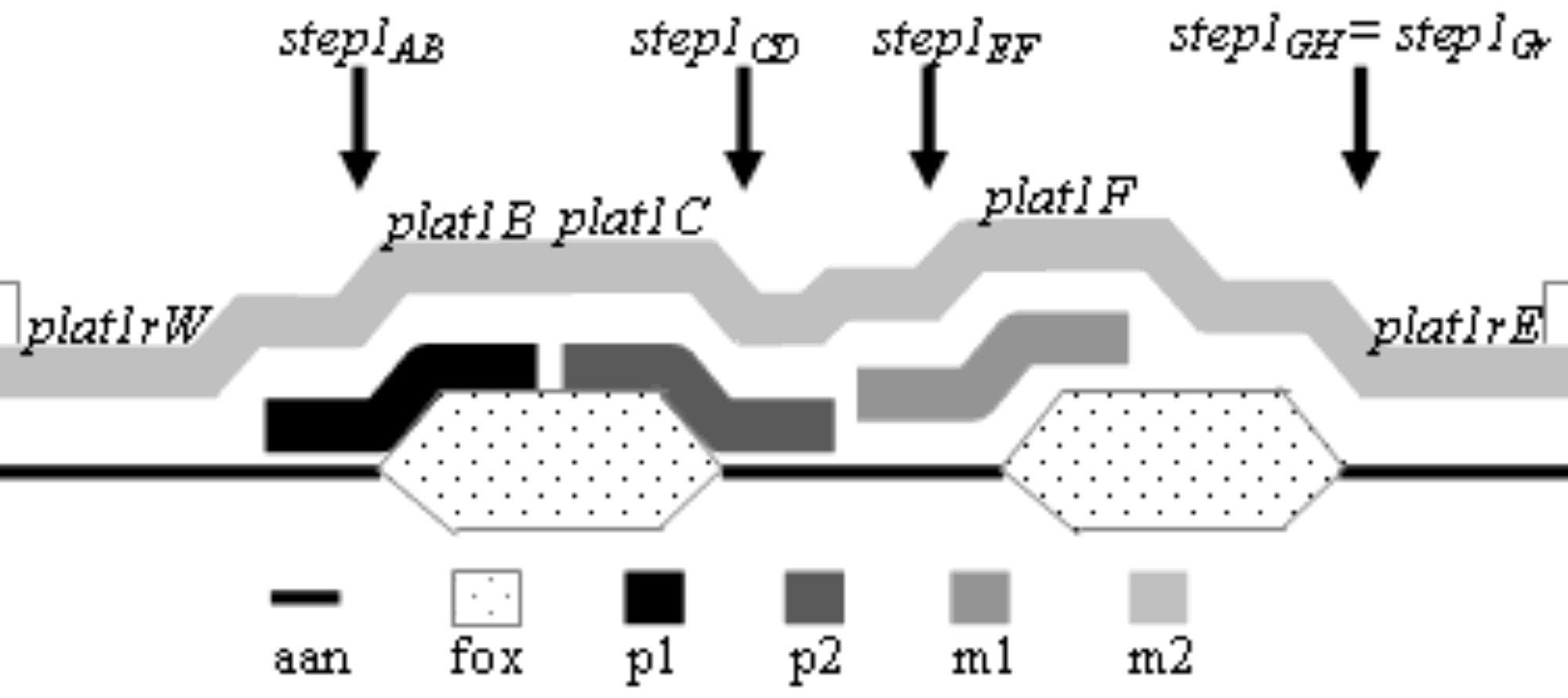
a)
b) Figure T.2.1.For thickness test structure
#1: a) a design rendition and b) a
cross-section.
To obtain the
measurements in this data sheet,
consult the following: [1] J. C.
Marshall and P. T. Vernier,
"Electro-physical Technique for
Post-fabrication Measurements of
CMOS Process Layer Thicknesses,"
NIST Journal of Research,
Vol. 112, No. 5, 2007, p.
223-256.
[2] SEMI MS2, "Test Method for Step
Height Measurements of Thin
Films."
date data taken (optional) =
/
/
fabrication
Preliminary
INPUTS
Data Set Prelims
Description
1
×
magnification
2
orient =
orientation of the test
structure on the test
chip
3
align =
alignment ensured ?
4
level =
data leveled ?
5
cert =
μm
6
σcert
=
μm
7
zrepeat(shs)
=
μm
at the same location on
the physical step height
(whichever is larger)
8
z6
=
μm
9
zdrift
=
μm
10
calz =
at the same location on
the physical step height
11
zperc
=
%
if
applicable, over the
instrument's total scan
range, the maximum
percent deviation from
linearity, as quoted by
the instrument
manufacturer (typically
less than 3%)
12
crystal =
%
13
sigma
=
TABLE
1a -
Calibrated
Step
Height Measurements
(in
Micrometers)*,**
#
Step
Height
uWstep
ucert
urepeat(shs)
udrift
ulinear
ucW
1
step1AB
2
step1CD
3
step1EF
4
step1GH
5
step1rA
6
step1rD
7
step1rE
8
step2rA
9
step2AB
10
step2BC
11
step2CD
12
step2BD
13
step3AB(0)
14
step3AB(n)-
15
step3BC(0)
16
step3CD(0)
*
Supply inputs to the columns
labeled "Height" and "uWstep." **
Where ucert =
|stepNXY|
σcert /
cert and urepeat(shs)
=
|stepNXY| zrepeat(shs) /
[2 (1.732)
z6]
and udrift =
|stepNXY|
(zdrift
calz)
/
[2 (1.732) cert] and ulinear =
|stepNXY| zperc /
(1.732)
and ucW
= (uWstep2
+ ucert2
+ urepeat(shs)2
+ udrift2
+ ulinear2)1/2 where
each standard uncertainty
component is obtained using
a Type B analysis, except
for uWstep,
which uses a Type A analysis.
TABLE
1b -
Calibrated
Step
Height Measurements from
Table 1a
(in
Micrometers)
with
Additional Uncertainty
Components*,**,***
[where
σrough
=
μm****]
#
Step
Height
σplatNX
σplatNY
ubasic
uWstep
uLstep
ures*****
uc
1
step1AB
2
step1CD
3
step1EF
4
step1GH
5
step1rA
6
step1rD
7
step1rE
8
step2rA
9
step2AB
10
step2BC
11
step2CD
12
step2BD
13
step3AB(0)
14
step3AB(n)-
15
step3BC(0)
16
step3CD(0)
*
Supply inputs for "σplatNX,"
"σplatNY,"
"ures,"
and "σrough." ** The values for
"Height" and "uWstep"
are taken directly from
Table 1a when the "Calculate
and Verify" button is
pushed. *** Where ubasic
= (ucert2
+ urepeat(shs)2
+ udrift2
+ ulinear2)1/2
and uLstep
= [(σplatNX
-
σrough)2
+ (σplatNY
-
σrough)2]1/2
and uc
= (ubasic2
+ uWstep2
+ uLstep2
+ ures2)1/2 where
each standard uncertainty
component is obtained using
a Type B analysis, except
for uWstep,
which uses a Type A analysis.
****Where
σrough
is the smallest of all the
values for
σplatNX
and
σplatNY
*****
Non-zero data can be added
to the column labeled "ures"
to obtain
En
values less than or equal to
1.0 in Tables 5 and 6.
TABLE
2 -
Oxide Thickness Values From
Capacitances*,**
[with
σε
=
(aF/μm)***
and
σresCa
=
(aF/μm2)***]
#
Thickness Designation
Ca
σCa***
ures
t
uc
(aF/μm2)
(aF/μm2)
(μm)
(μm)
(μm)
1
tfox(p1/sub)elec
2
tthin(p1/aan)elec
3
tfox(p2/sub)elec
4
tthin(p2/aan)elec
5
tthin(p2/p1)elec
6
[tfox,m1(pmd/sub)+tpmd(m1/fox)]elec
7
tpmd(m1/aan)elec
8
tpmd(m1/p1)elec
9
tpmd(m1/p2)elec
10
[tfox,m2(pmd/sub)+tpmd(imd/fox)
+timd(m2/pmd)]elec
11
[tpmd(imd/aan)
+timd(m2/pmd)]elec
12
[tpmd(imd/p1)
+timd(m2/pmd)]elec
13
[tpmd(imd/p2)
+timd(m2/pmd)]elec
14
timd(m2/m1)elec
*
Supply inputs for "Ca,"
"σCa,"
"σε,"
and "σresCa."
** Where
t = εSiO2
/ Ca with
εSiO2
= 34.5 aF/μm
and uc
= (uCa2
+ uε2
+ ures2)1/2 with uCa =
[εSiO2/ (Ca +
σCa)
-
εSiO2/ (Ca
-
σCa)] / 2
and uε= [(εSiO2+
3σε)
/ Ca
-
(εSiO2
-
3σε)
/ Ca
] / [2 (1.732)]
and ures
= σresCat
/ Ca where
each standard uncertainty
component is obtained using a
Type B analysis. ***
Non-zero data can be added
to "σresCa"
to obtain
En
values less than or equal to 1.0
in Tables 5 and 6.
Alternatively or in addition,
the value(s) for σε
and/or σCa
can be modified.
TABLE
3 -
Thickness Values For The
Interconnects*,**
#
Symbol
Rs
σRs***
ρ
σρ***
ures***
t
uc
(Ω/□)
(Ω/□)
(Ω-μm)
(Ω-μm)
(μm)
(μm)
(μm)
1
t(p1)elec
2
t(p2)elec
3
t(m1)elec
4
t(m2)elec
* Supply inputs to
the columns labeled
"Rs,"
"σRs,"
"ρ,"
"σρ,"
and "ures." ** Where t
=
ρ
/ Rs
and
uc = (uRs2
+ uρ2
+ ures2)1/2
with uRs
= [ρ/ (Rs
+
σRs)
-
ρ/ (Rs
-σRs)]
/ 2
and
uρ= [(ρ
+
3σρ)
/ Rs
-
(ρ
-
3σρ)
/ Rs
] / [2 (1.732)] where each
standard uncertainty component
is obtained using a Type B
analysis.
***
Non-zero data can be added to
the column labeled "ures"
to obtain En
values less than or equal
to 1.0 in Tables 5 and 6.
Alternatively or in addition,
the values for σRs
and/or σρ
can be modified.
TABLE
4 -
Crystal Lattice Percentages
#
Approach
%tab
(%)
%tbe (%)
1
Electrical*
2
Physical**
* A
prediction for the ideal
case **
As calculated from step1AB
in Table 1a and tfox(p1/sub)elec
and
tthin(p1/aan)elec
in Table 2
TABLE 5 -
Calculated Thickness Values
for the Given Thicknesses*,**
#
Thickness
Designation
tphys (μm)
uc,phys (μm)
telec
(μm)
uc,elec
(μm)
En***
En
< 1.0 ?
1
tfox(p1/sub)
2
tthin(p1/aan)
3
t(p1)
4
t(p1')
5
tfox(p2/sub)
6
tthin(p2/aan)
7
tthin(p2/p1)
8
t(p2)
9****
tfox,m1(pmd/sub)
10
tpmd(m1/fox)
11
tpmd(m1/aan)
12
tpmd(m1/p1)
13
tpmd(m1/p2)
14
tpmd(imd/fox)
15
tpmd(imd/aan)
16
tpmd(imd/p1)
17
tpmd(imd/p2)
18
tfox,m1(pmd/sub)+tpmd(m1/fox)
19
t(m1)
20****
tfox,m2(pmd/sub)
21
tpmd(imd/aan)+timd(m2/pmd)
22
tpmd(imd/p1)+timd(m2/pmd)
23
tpmd(imd/p2)+timd(m2/pmd)
24
timd(m2/pmd)
25
timd(m2/m1)
26
tfox,m2(pmd/sub)+tpmd(imd/fox)
+timd(m2/pmd)
27
t(m2)
28
timd(gl/pmd)
29
timd(gl/m1)
30
t(gl)
31
t(ni)
*
For use in calculations, choose
the thickness (either physical
or electrical) with the lower
value of uc. ** This analysis
assumes that [tpmd(imd/aan)+timd(m2/pmd)]phys=[tpmd(imd/aan)+timd(m2/pmd)]elec
and tpmd(m1/p1)phys=tpmd(m1/p1)elec. *** Where
En=
|tphys
- telec|
/
[sigma
(uc,phys2
+ uc,elec2)1/2]
if sigma
¹
10
and En
= |tphys
-
telec|
/ (3uc,phys+3uc,elec)
if sigma = 10.
For the above data,
sigma =
.
If sigma = 2
(recommended), then 95 % of the
data in Tables 5 and 6 should
have
En
values less than or
equal to 1.0. **** If
tfox(pmd/sub)
=
tfox,m1(pmd/sub)
= tfox,m2(pmd/sub),
then for the sample data tphys
for #9 is the thickness to
use in calculations due to it
having the lower value of uc.
TABLE
6 -
Calculated Thickness Values
For The Virtual Oxides*
#
Thickness
Designation
tphys (μm)
uc,phys (μm)
telec
(μm)
uc,elec
(μm)
En**
En
< 1.0 ?
1
tthin,be(p1/aan)
2
tthin,ab(p1/aan)
3
tthin,be(p2/aan)
4
tthin,ab(p2/aan)
5
tthin,be(p2/p1)
6
tthin,ab(p2/p1)
7
tfox,be(p1/sub)
8
tfox,ab(p1/sub)
9
tfox,ab(p2/sub)
10
tfox,ab,m1(pmd/sub)
11
tfox,ab,m2(pmd/sub)
* For use in
calculations, choose the
thickness (either physical or
electrical) with the lower value
of uc. ** Where
En=
|tphys
- telec|
/
[sigma (uc,phys2
+ uc,elec2)1/2]
if sigma
¹
10 and
En
=
|tphys
-
telec|
/
(3uc,phys+3uc,elec)if sigma = 10.
For the above data,
sigma =
.
If sigma = 2
(recommended), then 95 % of the
data in Tables 5 and 6 should
have
En
values less than or
equal to 1.0.
Results for number of
En values less
than or equal to 1.0 in Tables 5
and 6 with
sigma = :
number of "yeses" =
percent "yeses"=
%
number of "nos" =
percent "nos"=
%
total
number of "yeses" and "nos" =
total =
%
Report the results as follows: Since it can be assumed that the
estimated values of the
uncertainty
components are
approximately uniformly
or Gaussianly distributed with
approximate combined standard
uncertainty
uc, the
thickness is believed to lie
in the interval t
±
uc (expansion factor
k=1) representing a
level of confidence of
approximately 68 %.
Modify the input data,
given the information
supplied in any flagged
statement below, if
applicable, then
recalculate:
1.
2.
3.
4.
5.
6.
7.
8.
calz
and (cert
+ 0.100 μm)/calz.
9.
10.
11.
12.
13.
14.
15.
16.
σrough
for Table 1b should be between
0.0000 μm and the smallest value
for
σplatNX
and
σplatNY,
inclusive.
17.
18.
19.
ε
for Table 2 should be
between 0.0 aF/μm
and 0.3 aF/μm,
inclusive.
20.
σresCa
for Table 2 should be
between 0 aF/μm2and
3.0 aF/μm2,
inclusive.
21.
22.
23.
Ω/□
and 35.0
Ω/□
for t(p1)elec
and t(p2)elec
and between
0.0100
Ω/□
and 0.0700
Ω/□
for t(m1)elec
and t(m2)elec.
24.
25.
ρ
in Table 3 should be
between 5.0
Ω-μm
and 10.0
Ω-μm
for t(p1)elec
and t(p2)elec
and between
0.020
Ω-μm
and 0.040
Ω-μm
for t(m1)elec
and t(m2)elec.
26.
27.
28.
29.
30.
31.
There are
thicknesses with En
values greater than 1.0
in Tables 5 and/or 6
with
sigma
=
.
Is this ok?