PML Banner
 
Data Analysis Sheet T.1

Data analysis sheet for composite oxide thickness measurements in a
commercial CMOS process for use with the MEMS 5-in-1 (RM 8096).
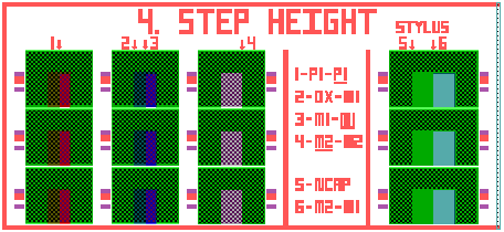
Top view of step height test structures on CMOS 5-in-1 test chip.                                                                     
Figure T.1.1.  Top view of step height test structures on a MEMS 5-in-1 RM.

To obtain the measurements in this data sheet, consult the following:
[1] J. C. Marshall and P. T. Vernier, "Electro-physical Technique for Post-fabrication
Measurements of CMOS Process Layer Thicknesses," NIST Journal of Research,
Vol. 112, No. 5, 2007, p. 223-256.
[2] SEMI MS2, "Test Method for Step Height  Measurements of Thin Films."


date (optional) = / /


comments (optional) =
 
TABLE 1 - Calibrated Step Height MEASUREMENTS*
# Step #** Step*** step height****

ucSH****

ures

ucstep*****
(μm) (μm) (μm) (μm)
1 1 H=step1AB  
2 2 D=step2rA
3 3 F=step1EF
4 4 J=step1GH
5 5 E=step3AB(n)-
6 6 C=step3BC(0)

* Supply inputs to the columns labeled "step height," "ucSH," and "ures."
** The step number as labeled in Fig. T.1.1.
***
The corresponding step for the test structures used with Data Sheet T.2.
**** These inputs can be obtained from Data Sheet SH.1.a.

***** Where ucstep = (ucSH2 + ures2)1/2
       
 (where ures is a Type B component that is typically set equal to 0)


TABLE 2 - Oxide Thickness Values From Capacitances
*,**
[with σε =
aF/μm]

#*** Thickness Designation Ca σCa σresCa/rres t uctCa
(aF/μm2) (aF/μm2)   (μm) (μm)
1 G=tfox(p1/sub)elec
2 I=tthin(p1/aan)elec
6 K=[tfox,m1(pmd/sub)+tpmd(m1/fox)]elec
7 L=tpmd(m1/aan)elec
10 M=[tfox,m2(pmd/sub)+tpmd(imd/fox)

+timd(m2/pmd)]elec

11 A=[tpmd(imd/aan) +timd(m2/pmd)]elec
* Supply inputs for "Ca," "σCa," "σε," and "σresCa/rres."
** Where t = εSiO2 / Ca with εSiO2 = 34.5 aF/μm
and uctCa = t [(σε / εSiO2)2 + (σCa / Ca)2 + (σresCa / rres)2]1/2
where each standard uncertainty component is obtained using a Type B analysis
with σresCa/rres typically set equal to 0.
*** The numbering in this table corresponds to the numbering for the corresponding thicknesses
in Table 2 of Data Sheet T.2.


TABLE 3 - Thickness Values For The Interconnects*,**

# Symbol Rs σRs ρ σρ σresRs / rres t uctRs
(Ω/□) (Ω/□) (Ω-μm) (Ω-μm)   (μm) (μm)
1

B=t(m2)elec

* Supply inputs to the columns labeled "Rs," "σRs," "ρ," "σρ," and "σresRs / rres."
** Where t = ρ / Rs
and uctRs = t [(σρ / ρ)2 + (σRs / Rs)2 + (σresRs / rres)2]1/2
where each standard uncertainty component is obtained using a Type B analysis
with σresRs/rres typically set equal to 0.


TABLE 4 - Oxide Thickness Calculation

# Symbol t uc
(μm) (μm)
1 O=G-H+HI / (I-G)
2 X=B+C-D+E         
3 Y1=M    
4 Y2=A+K-L    
5 Y3=A-J+O    
6 Y4=A+F+O
7 Z1=X+Y1    
8 Z2=X+Y2    
9 Z3=X+Y3    
10 Z4=X+Y4  
11  

Uoxide = 2ucoxide = μm     (expanded uncertainty)
3ucoxide = μm
toxide - Uoxide = μm  (a lower bound for toxide)
toxide
+ Uoxide =
μm  (an upper bound for toxide)

Report the results as follows
:  If it is assumed that the estimated values of the uncertainty
components are approximately Gaussianly distributed with approximate combined standard
uncertainty ucoxide, the oxide beam thickness is believed to lie in the interval toxide ± ucoxide 
(expansion
factor k=1) representing a level of confidence of approximately 68 %. 


Modify the input data, given the information supplied in any flagged statement below, if applicable, then recalculate:

1.
2.
3.
4.
5. σε  for Table 2 should be between 0.0 aF/μm and 0.3 aF/μm, inclusive.
6. The values for Ca in Table 2 should be between 1.0 aF/μm2 and 1300.0 aF/μm2.
7. The values for σCa in Table 2 should be between 0.00 aF/μm2 and 10.00 aF/μm2.
8. The values of σresCa/rres in Table 2 should be between 0 and 0.05, inclusive.
9. Ω/ and 0.0700 Ω/ .
10.   σRs in Table 3 should be between 0.0001 Ω/ and 0.0050 Ω/.
11. ρ in Table 3 should be between 0.020 Ω-μm and 0.040 Ω-μm.
12.
13.
14.
15.

Return to Main MEMS Calculator Page.

Email questions or comments to mems-support@nist.gov.

NIST is an agency of the U.S. Commerce Department.
The Semiconductor and Dimensional Metrology Division is within the Physical Measurement Laboratory.
The MEMS Measurement Science and Standards Project is within the Nanoscale Metrology Group.

Date created: 1/12/2009
Last updated:
4/26/2013