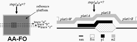
Data
analysis sheet for step height
measurements taken during the
same data session from two
step height test structures.
a)
b)
Figure SH.2.1.For a CMOS step height test
structure: a) a design rendition and
b) a cross-section.
To obtain the
following measurements, consult SEMI
standard test method MS2 entitled
"Test Method for Step Height
Measurements of Thin Films."
date data taken (optional) =
/
/
Table 1 - Preliminary
INPUTS
First Test Structure
Second Test Structure
Description
1
proc =
which process?
2
which =
For CMOS SRM chips,
which test structure?
For MUMPs chips, which
quad?
3
which2 =
Which platform, where
"first" corresponds to
the leftmost or
bottommost platform in
the test structure, counting the reference
platform?
4
which3 =
For CMOS chips, which
iteration of the test
structure where "first"
corresponds to the
topmost test structure
in the column?
5
orient =
orientation of the test
structure on the test
chip
6
×
magnification
7
align =
alignment ensured?
8
level =
data leveled?
9
cert =
μm
10
σcert
=
μm
11
zrepeat(shs)=
μm
at the same location on
the physical step height
(whichever is larger)
12
z6
=
μm
13
zdrift
=
μm
14
calz
=
15
zperc
=
%
16
σroughLX=
μm
σplatLXt.
(However, if the
surfaces of platLX,
platMY, platLr
, and platMr all
have identical
compositions, then it is
measured as the smallest
of all the values
obtained for
σplatLXt,
σplatMYt,
σplatLrDt,
and
σplatMrDt
in which case
σroughLX
=
σroughMY.)
17
σroughMY=
μm
σplatMYt.
(However, if the
surfaces of platLX,
platMY, platLr
, and platMr all
have identical
compositions, then it is
measured as the smallest
of all the values
obtained for
σplatLXt,
σplatMYt,
σplatLrDt,
and
σplatMrDt
in which case
σroughLX
=
σroughMY.)
Nomenclature:
"L" and "M" refer
to the test structure number ("1,"
"2," "3," etc.),
"X" and "Y" refer
to the platform letter ("A,"
"B," "C," etc.),
"r" refers to the
reference platform,
"D" directionally
indicates which reference
platform ("N," "S,"
"E," or "W"), and
"t" indicates which data
trace ("a," "b,"
or "c").
Table 2a - Uncalibrated
REFERENCE PLATFORM
INPUTS
(in
μm)
First Test Structure
Second Test Structure
1a
4a
1b
4b
2a
5a
2b
5b
3a
6a
3b
6b
Table 2b - Calibrated
REFERENCE PLATFORM
CALCULATIONS
(in
μm)
First Test Structure
Second Test Structure
7a
8a
7b
8b
Note 1:
platLr = AVE(platLrWa,
platLrWb, platLrWc, platLrEa,
platLrEb, platLrEc) calz
Note 2:
splatLr = STDEV(platLrWa,
platLrWb, platLrWc, platLrEa,
platLrEb, platLrEc) calz
Note 3: The calculations
for the second test structure
are similar to the calculations
for the first test structure
given in Notes
1 and 2.
Table 3a - Uncalibrated
PLATFORM INPUTS
(in
μm)
First Test Structure
Second Test Structure
9a
9b
10a
10b
11a
11b
12a
platLXa
=
12b
platMYa
=
13a
platLXb
=
13b
platMYb
=
14a
platLXc
=
14b
platMYc
=
Table 3b - Calibrated
PLATFORM CALCULATIONS
(in
μm)
First Test Structure
Second Test Structure
15a
15b
16a
16b
17a
platLXave
=
17b
platMYave
=
18a
18b
19a
19b
20a
20b
21a
21b
22a
22b
23a
23b
24a
24b
Note 4:
platLX = calz AVE(platLXa,
platLXb, platLXc)-
platLr
Note 5:
splatLX =
calz STDEV(platLXa,
platLXb, platLXc)
Note 6:
σplatLXave = calz AVE(σplatLXa,
σplatLXb,
σplatLXc)
Note 7:uLplatLX
=
σplatLXave
-
calz
σroughLX
Note 8:
uWplatLX = SQRT(splatLX2+splatLr2)
Note 9:
ucertLX = |σcertplatLX
/ cert|
Note 10:
urepeat(shs)LX
= |zrepeat(shs)platLX
/ [2(1.732) z6]|
Note 11:
udriftLX = |(zdriftcalz) platLX
/ [2(1.732)cert]|
Note 12:
ulinearLX
= |zpercplatLX
/ (1.732)|
Note 13:
uplatLX = SQRT(uLplatLX2+uWplatLX2+ucertLX2+urepeat(shs)LX2+udriftLX2+ulinearLX2)
(Each of the standard
uncertainty components is
obtained using a Type B
analysis,
except for uWplatLX,
which uses a Type A analysis.)
Note 14: The
calculations for the second test
structure are similar to the
calculations for the first
test structure given in Notes
4 through 13, inclusive.
Table 4 - Calibrated
OUTPUTS
(in
μm)
25
Note 15:
stepLXMY
= platMY-platLX
Note 16:
ucSH =
SQRT(uplatLX2+uplatMY2)
Note 17: The
numerical values of the sample
platform inputs in Data Sheet
SH.1 are identical to the
numerical values of the sample
platform inputs in this data
sheet. The resulting
values for stepNXY
in Data Sheet SH.1 and stepLXMY
in this data sheet are
comparable, yet the value for
ucSH
in this data sheet is larger
than the ucSH
value in Data Sheet SH.1.
This implies that step height
measurements from one step
height test structure (as
calculated in Data Sheet SH.1)
are preferred to step height
measurements from two step
height test structures (as
calculated in this data sheet).
Report the results as follows: Since it can be assumed that the
estimated values of the
uncertainty
components are
approximately uniformly
or Gaussianly distributed with
approximate combined standard
uncertainty
ucSH, the step
height is believed to lie in the
interval stepLXMY
±
ucSH (expansion
factor k=1)
representing a level of
confidence of approximately 68 %.
Modify the input data,
given the information
supplied in any flagged
statement below, if
applicable, then
recalculate:
1.
2.
3a.
3b.
4a.
4b.
5.
6.
7.
8.
calz.
9.
10.
11.
12.
σroughLX
and
σroughMY
should be greater than
0.0
μm
and less than or equal
to the smallest measured
value for
σplatLXt
and
σplatMYt,
respectively.
13.
14.
15.
16.
17.
18.
19.
20.
21.
σplatLXt
and
σplatMYt
should be between 0.0
μm and 0.02
μm, inclusive.